Description
The SNx4HC595 devices contain an 8-bit, serial-in, 1 shift register that feeds an 8-bit D-type storage register. The storage register has parallel 3-state outputs. Separate clocks are provided for both the shift and storage register. The shift register has a direct overriding clear (SRCLR) input, serial (SER) ICC input, and serial outputs for cascading. When the output-enable (OE) input is high, the outputs are in the high-impedance state.
Features
• 8-Bit Serial-In, Parallel-Out Shift parallel-out
• Wide Operating Voltage Range of 2 V to 6 V
• High-Current 3-State Outputs Can Drive Up to 15 LSTTL Loads
• Low Power Consumption: 80-μA (Maximum)
• tpd = 13 ns (Typical)
• ±6-mA Output Drive at 5 V
• Low Input Current: 1 μA (Maximum) Device Information(1)
• Shift Register Has Direct Clear
• On Products Compliant to MIL-PRF-38535, All Parameters Are Tested Unless Otherwise Noted. On All Other Products, Production Processing Does Not Necessarily Include Testing of All Parameters.
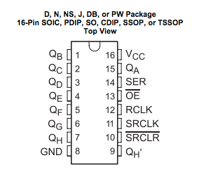
Pins
| Pin | Description |
|---|---|
| QA-QH | Data Output |
| SER | Serial Data Input |
| OE | Output Enabled (Active Low) |
| RCLK (Latch) | Register Clock Input |
| SRCLK (Clock) | Shift Register Clock Input |
| SRCLR | Shift Register Clear (Active Low) |
Arduino Example Code
//Define PinModes
pinMode (latchPin,OUTPUT);
pinMode (dataPin, OUTPUT);
pinMode (clkPin, OUTPUT);
pinMode (oePin, OUTPUT);

//disable output on SR
digitalWrite(oePin,HIGH);

//define data
byte data = 0;


//set or clear bits in our byte variable data
bitSet(data,bitToSet);
bitClear(data,bitToClear);


//write out to SR
digitalWrite(latchPin,LOW);
shiftOut(dataPIn,clockPin,LSBFIRST,data);
digitalWrite(latchPin,HIGH);


//Enable output on SR
digitalWrite(oePin,LOW);
References
| Reference | URL |
|---|---|
| Datasheet | http://www.ti.com/lit/ds/symlink/sn74hc595.pdf |
| Shift Register Tutorial | https://learn.sparkfun.com/tutorials/shift-registers?_ga=2.36116968.935449524.1518383708-1496492250.1516240716 |