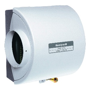
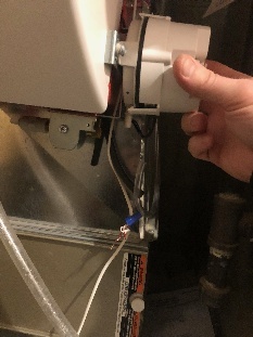
Controller
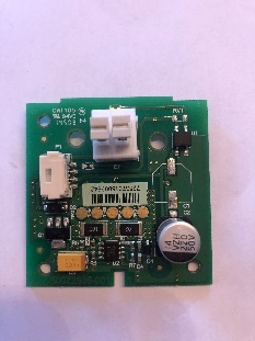
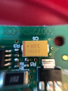
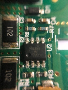
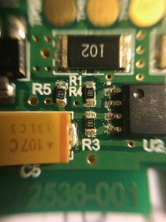
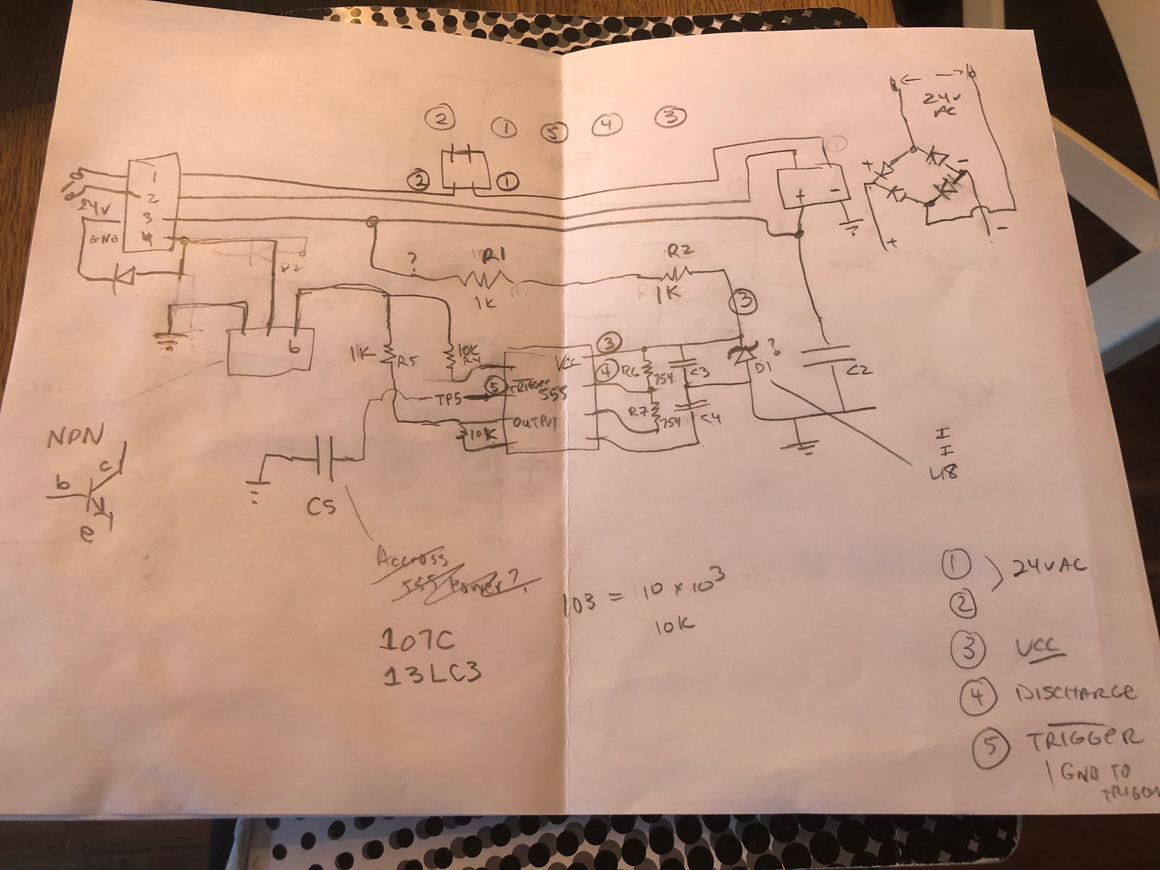
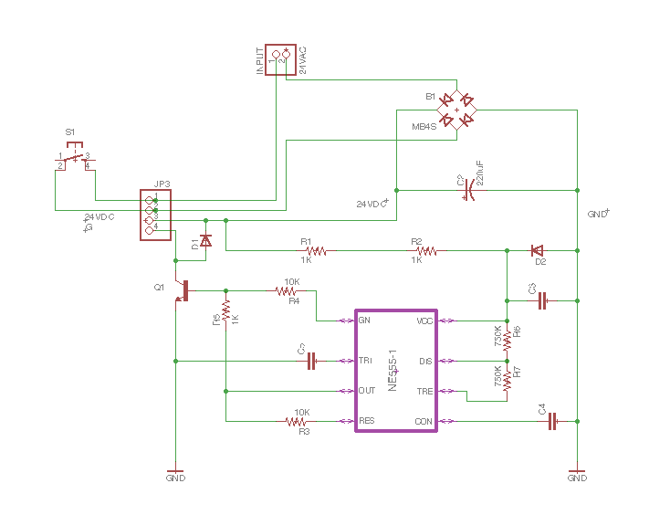
Schematic
Here is the schematic that I put together based on some testing.
Based on this schematic, I'm thinking that the transistor Q1 is bad. You would think that the GND pin on the 555 would go to ground via a pullup and that would be that.
Other thoughts:
- D2 is a zener diode which acts as a voltage regulator for the 555 chip.
References
| Reference | URL |
|---|---|
| 555 Timer | http://www.ti.com/lit/ds/symlink/lmc555.pdf |